------How to achieve precision electrostatic protective packaging with fast delivery and optimized structures.
Introduction:
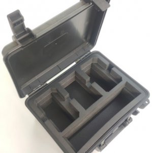
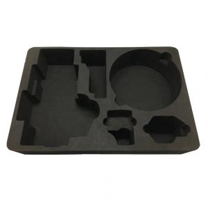
In electronics manufacturing and semiconductor industries, protecting sensitive components requires more than just the material's electrostatic dissipative properties—it demands a precise, reliable physical space. Thick-gauge thermoformed trays have become the preferred choice for transporting and storing PCBs, precision modules, and other components due to their excellent structural strength and protective capabilities.
However, when facing challenges such as rapid product iterations, tight deadlines, and the need for high-density layouts, balancing speed with precision becomes critical for engineers. Recently, we completed a challenging project for a client (name confidential per request) that perfectly demonstrates our expertise in thick-gauge thermoforming. Here is our professional experience sharing.
1. Speed: One-Week Turnaround from Drawing to Delivery
In the fast-paced electronics industry, time is money. Traditional steel molds or CNC machining cycles are too long to meet prototyping or urgent order requirements.
Our Advantage: Leveraging our in-house mold shop and material inventory, we can complete the entire process—from mold design and fabrication to finished product delivery—within one week. This critical capability ensures clients can quickly validate product designs or respond to unexpected production capacity needs
2. Material: Flexible Options with ESD HIPS and PET
Not all ESD requirements are the same. Material selection is crucial based on product sensitivity and application environment.
Our Solution: We offer both ESD HIPS and ESD PET material options. HIPS is easier to form, suitable for products with complex structures and deeper draws, while PET offers better heat resistance and mechanical strength. Like our machined, the anti-static properties of these materials are volume conductive (carbon powder filled), with stable resistance values of 10⁶−10⁹ Ω. The ESD performance remains consistent even after deep drawing.
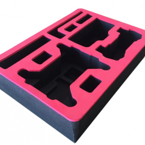
3. Design Breakthrough: High Capacity in a Compact Footprint
The core challenge of this project was: accommodate 32 vertical insertion slots for PCBA within a compact tray size of just 280*180*58mm, using 2.2mm thick material.
Professional Insight:
Typically, a 58mm depth with 2.2mm thick-gauge material represents a significant draw ratio, corner thinning or slot deformation.
Our Solution: By optimizing the mold's draft angles and radius designs, combined with stress-relieving forming techniques, we successfully achieved this high-density, deep-draw vertical slot structure. Each slot maintained precise dimensions and sufficient rigidity, ensuring stable and reliable PCBA insertion and transport without the common issues of warping or spring-back.
4. Maintaining ESD Integrity Through Processing
A common misconception is that deep drawing destroys the material's anti-static network.
Our Assurance: Because our ESD HIPS and PET materials are fully modified throughout—with anti-static carbon chains distributed within the entire sheet—even a deep draw of 58mm on 2.2mm material (which does cause physical wall thickness variations) leaves the volume resistivity unchanged. We consistently ensure the ESD performance of the entire tray meets industry standards across all areas.
5. Dimensional Stability and Tolerance
Plastic thermoforming isn't as absolutely precise as metal stamping, but we can control variables through experience.
Our Advice: During design and acceptance, the natural shrinkage of thermoformed parts must be considered. We pre-compensate for this during the mold design phase, ensuring final products stabilize at room temperature for 24 hours while maintaining dimensions within the specified tolerances.
Conclusion:
High-performance ESD thick-gauge thermoformed trays represent the perfect fusion of design intelligence and process experience. Whether meeting the challenge of a one-week delivery or tackling complex structures with deep slots and high density, our engineering team can provide the optimal solution for you.
✅ Call to Action
Looking for reliable ESD protective packaging for your precision PCBA or sensitive components? Need support with rapid prototyping and high-quality volume production?
Contact us today to receive specifications and a quotation within 24 hours.
�� Contact Us
YUFA Polymer Products Co., Ltd.
�� Address: Shenzhen, China
�� Email: info@yufapolymer.com
�� Web: www.yufapolymer.com